
Ultra-Fast Switching
≤200 ns frequency transitions support agile waveform and multi-frequency scheduling.
Less retuning delay leaves more of the operating window available for useful RF activity.
1.25–40 GHz ULTRA-FAST FREQUENCY-AGILE SOURCE
1.25–40 GHz
Output Frequency
≤200 ns
Frequency Switching
A compact microwave frequency synthesizer delivering ≤200 ns frequency switching, 0.1 MHz tuning resolution and low phase noise for agile radar front ends, EW research and high-speed RF test systems.
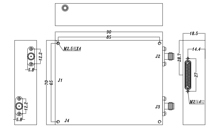
Mechanical integration drawing
90 × 70 × 18.5 mm
WHY SWITCHING SPEED MATTERS
Frequency switching speed determines how quickly a radar or RF system can transition between frequency states. Reducing switching time helps minimize retuning dead time and enables more agile waveform scheduling within a fixed operating window.
Reference switching interval
50 μs
This module
≤200 ns
Result
Up to 250×
shorter switching interval
In simple terms
The less time the system spends changing frequency, the more time it can spend transmitting, receiving and responding to changing signal conditions.
Illustrative comparison based on a 50 μs reference interval. Frequency switching time is only one component of total radar scan and track-update performance.
ENGINEERED FOR WIDEBAND AGILITY
Verified RF performance is paired with clear integration interfaces for radar, electronic-warfare research and high-speed microwave test architectures.
≤200 ns frequency transitions support agile waveform and multi-frequency scheduling.
Less retuning delay leaves more of the operating window available for useful RF activity.
Continuous 1.25–40 GHz output supports multi-band radar, microwave and RF test architectures.
One compact source can serve a broad range of development and integration requirements.
0.1 MHz tuning steps provide precise frequency planning and repeatable control.
Engineering teams gain finer control over channel placement and test repeatability.
≤−110 dBc/Hz at 1 kHz offset and 10 GHz supports signal purity in demanding radar and measurement chains.
A cleaner source helps protect measurement quality and waveform integrity.
A 90 × 70 × 18.5 mm module operating from −55°C to +85°C for space-constrained and harsh-environment systems.
The compact envelope simplifies installation where space and environmental margins are limited.
APPLICATION SCENARIOS
The module supplies fast, wideband frequency generation inside compliant research, test and system-integration environments.
Fast frequency generation for agile radar waveform and exciter architectures.
Supports radar research requiring rapid switching across wide frequency ranges.
Wideband, fast-hopping signal generation for controlled laboratory and system validation environments.
A compact source for radar transmitter, receiver and frequency-conversion chains.
Suitable for automated measurement, component characterization and wideband test platforms.
Integration into specialist microwave equipment and high-end measurement products.
HOW IT INTEGRATES
Designed for deterministic integration through parallel frequency addressing, trigger control and lock-status monitoring.
RF signal path
100 MHz Reference Input
Ultra-Fast Frequency-Agile Source
1.25–40 GHz RF Output
Radar Transceiver / RF Test Chain
Control path
System Controller
D18–D0, 3.3 V Logic + TRIG
Ultra-Fast Frequency-Agile Source
LDOUT Lock Status Feedback
Complete pin definitions are reserved for the full engineering datasheet.
TECHNICAL SPECIFICATIONS
Values below are reproduced from the supplied product document. Complete pin definitions remain available through an engineering review.
| Output Frequency | 1.25–40 GHz |
|---|---|
| Frequency Step | 0.1 MHz |
| Frequency Switching Time | ≤200 ns |
| Output Power | 3–8 dBm |
| Phase Noise | ≤−110 dBc/Hz @ 1 kHz offset, 10 GHz |
| Spurious, 1.25–20 GHz | ≤−66 dBc, typical |
| Spurious, 20–40 GHz | ≤−60 dBc, typical |
| Second-Harmonic Level | ≤−10 dBc |
| 1/2 and 3/2 Harmonic Level, 20–40 GHz | ≤−50 dBc |
| Reference Frequency | 100 MHz |
|---|---|
| Reference Input Power | 4 ± 2 dBm |
| Reference Phase Noise | ≤−160 dBc/Hz @ 1 kHz offset |
| Frequency Address | D18–D0, 3.3 V logic |
|---|---|
| Trigger | 3.3 V rising-edge trigger |
| Lock Detect | 2.7–3.5 V locked; ≤0.2 V unlocked |
| Reference Connector | Removable SMA |
| RF Connector | Removable K-type |
| Debug Interface | SMP |
| Supply | +6 V |
|---|---|
| Current | ≤1.8 A |
| Dimensions | 90 × 70 × 18.5 mm |
| Operating Temperature | −55°C to +85°C |
| Storage Temperature | −55°C to +100°C |
Expand a group to review its parameters.
| Output Frequency | 1.25–40 GHz |
|---|---|
| Frequency Step | 0.1 MHz |
| Frequency Switching Time | ≤200 ns |
| Output Power | 3–8 dBm |
| Phase Noise | ≤−110 dBc/Hz @ 1 kHz offset, 10 GHz |
| Spurious, 1.25–20 GHz | ≤−66 dBc, typical |
| Spurious, 20–40 GHz | ≤−60 dBc, typical |
| Second-Harmonic Level | ≤−10 dBc |
| 1/2 and 3/2 Harmonic Level, 20–40 GHz | ≤−50 dBc |
WHO IT IS FOR
Counter-UAS and frequency-agile radar manufacturers
Radar and defense-electronics system integrators
EW and frequency-hopping test-system developers
RF and microwave instrument manufacturers
Radar transceiver and frequency-source suppliers
Research institutes and advanced RF laboratories
FREQUENTLY ASKED QUESTIONS
ENGINEERING REVIEW
Share your operating band, hop profile, interface requirements and project timeline. Our engineering team will review product fit and integration requirements.